This is the first of a 4-part series describing the journey taken to hack this little device, an 8 port NVR for security cameras. In this part, we will take a look at (and inside) the device. In part 2 we will take a look at the firmware. Part 3 will have us port Doom to it. Finally, we will hack the built-in UI to give us a decent launcher for Doom.
The Device
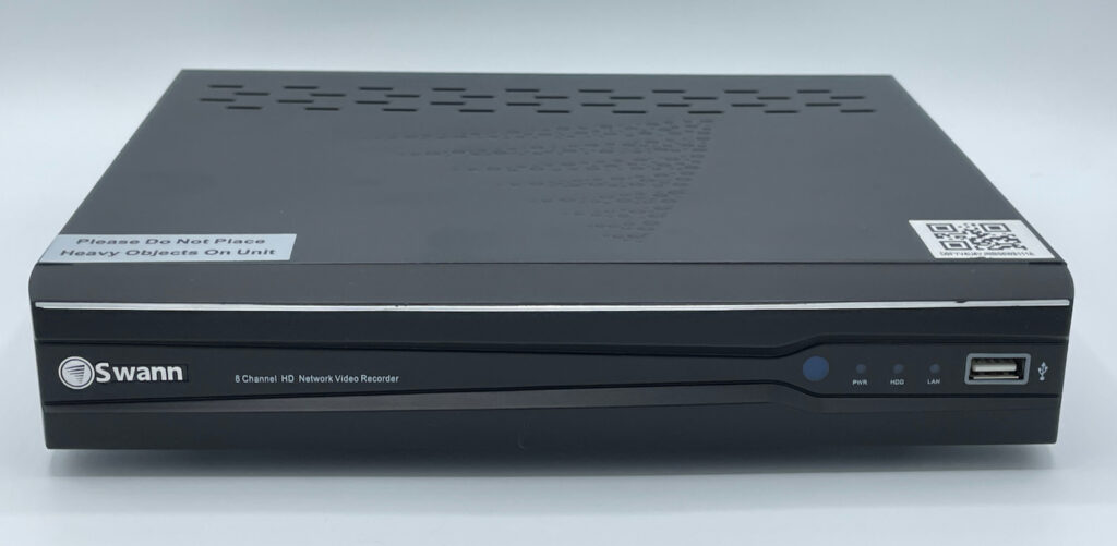
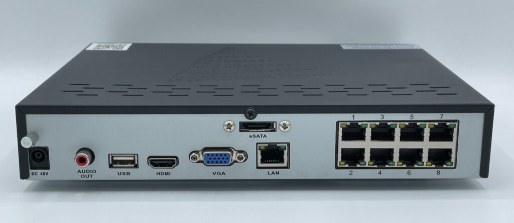
The Swann NVR8-7300 (also known as the Swann SRNVR-87300H) is an older security camera NVR (Network Video Recorder) that came to market around 2015. It has 8 channels capable of recording 3MP/30fps feeds from digital cameras (“IP Cameras”), and stores the H264-encoded video streams onto an internal hard drive of 2TB. It can power the cameras directly via their ethernet cable using PoE (Power over Ethernet). The device can be used on its own connected to an HDMI TV (or a VGA monitor), or it can be connected to a local network (LAN) via a cable (no Wifi) and used through apps on phones / PCs / Macs. Most commonly the device was sold as a bundle with 4 or 8 3MP “bullet” cameras. As of 2021 the device is discontinued.
Specs from the manufacturer:
- 8 Channels at 3MP, encoded in H264 (2048 x 1536 (4:3), 2304 x 1296 (16:9)), up to 30 frames per second (30 fps)
- Supports recording & replaying audio
- Storage: 2TB internal, upgradable to 6TB (3TB internal, 3TB external via eSata)
- 1Gbps ethernet port for LAN connectivity
- 8x100Mps PoE ethernet ports for 8 Cameras
- HDMI and VGA output, 1080p output resolution maximum
- 2 USB 2.0 ports (comes with a USB optical mouse)
- 48V DC power input, supplied by an external power supply (included)
- Dimensions: 10” x 9.0” x 2.0” / 255 x 230 x 51mm
The Insides
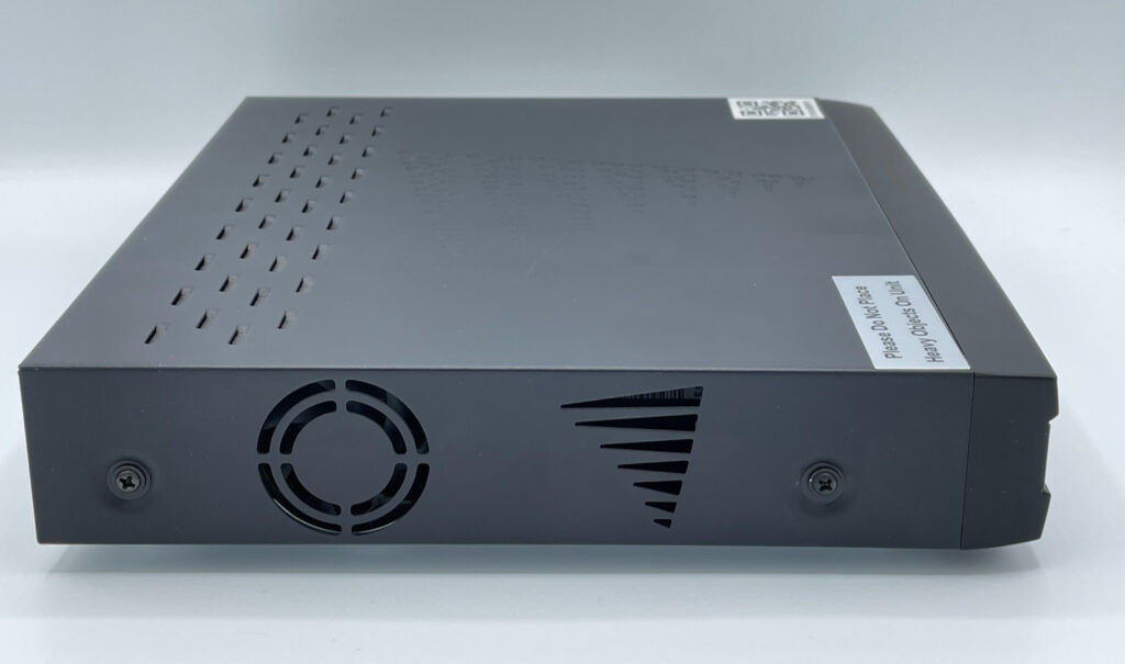
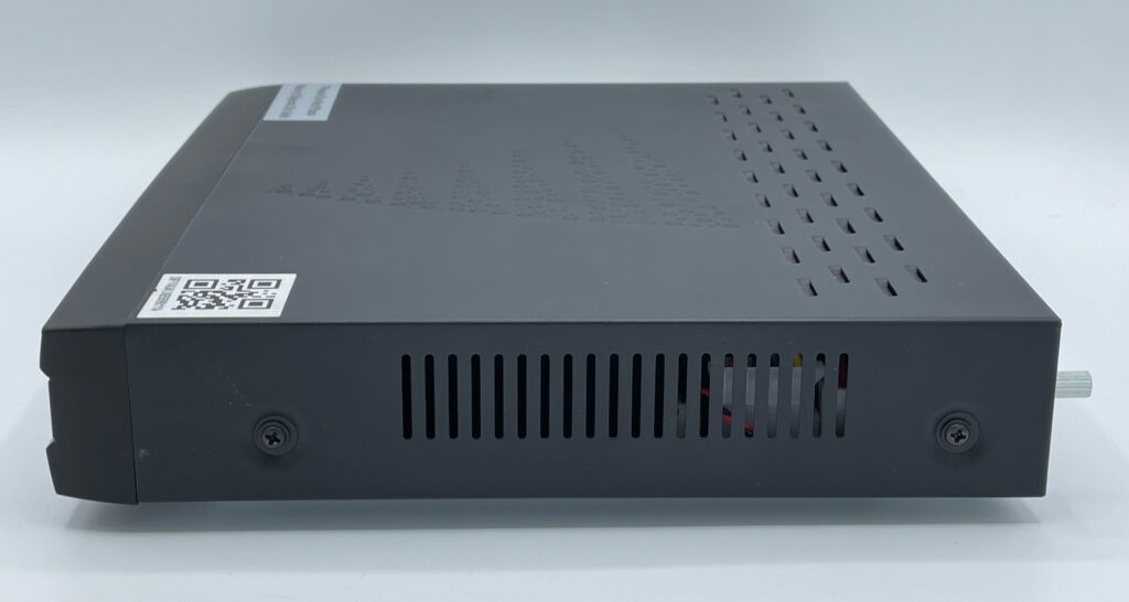
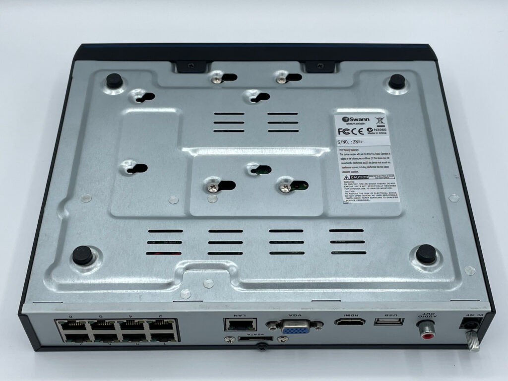
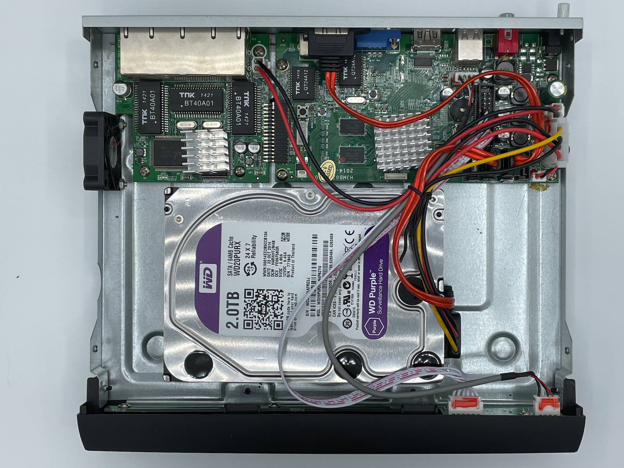
Opening the NVR is as simple as removing five screws (two on each side, one at the back) and removing the top cover. Once removed, the cover reveals a pretty simple design: a single-board computer with all the I/O ports, connected to a daughter board for the 8 PoE ethernet ports, and a standard, 3.5″ hard drive. A little fan standing on the left side keeps the air moving through the box, and a couple of cables run to the front panel for the front USB port a and the few LEDs there.
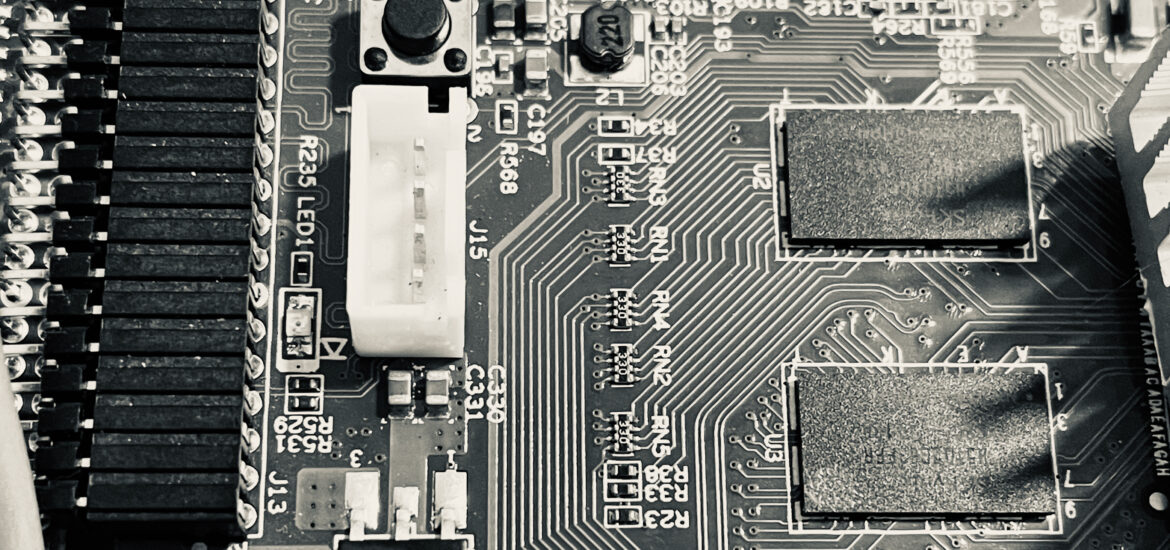
PCB: Main board (SBC)
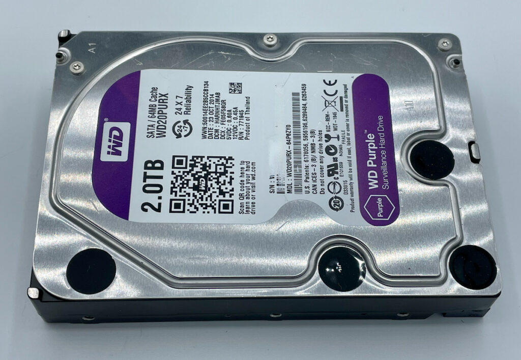
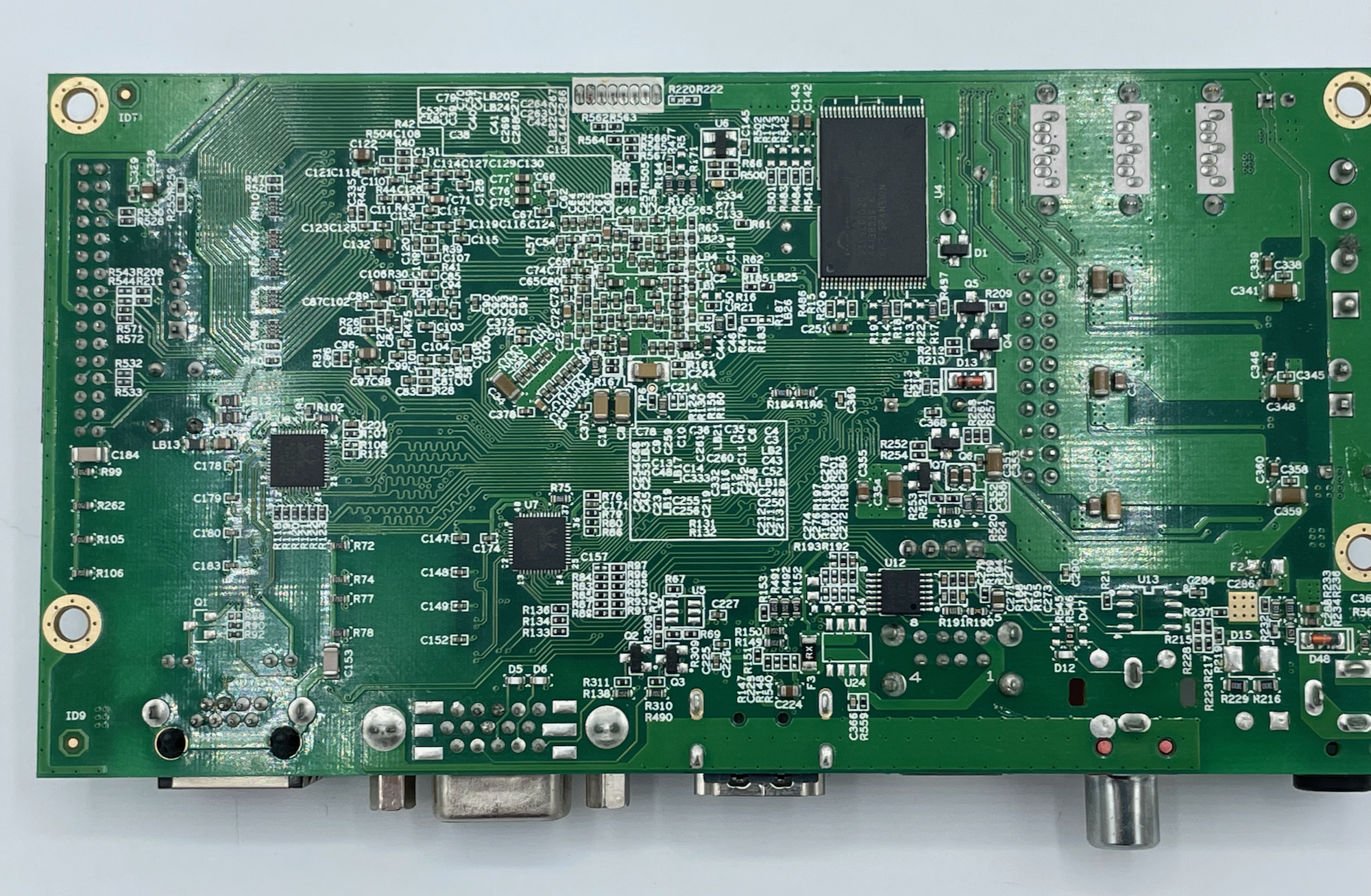
The main board PCB is that of the computer driving the NVR. It’s a Single Board Computer (SBC) architected around the HiSilicon Hi3535 SoC (System on a Chip). (HiSilicon is a subsidiary of Huawei that makes chips). This chip does pretty much everything: ARM Cortex A9 dual-core 1GHz for the brains, H264 hardware decoders and encoder, audio/video interfaces (VGA, HDMI, BT.1120 even), 2 gigabit ethernet ports, SATA, USB, I2S, I2C, GPIO, and various memory interfaces. The board uses two SKhynix 2Gb (i.e. 256MB) DDR3-1600 SDRAM modules for a total of 512MB of memory, and one Spansion 1Gb (128MB) SLC NAND Flash for the firmware (bootloader, OS, app, configuration). The video footage is stored off-board on the 3.5″ hard drive.
The board uses both network interfaces of the main chip. One is connected to the external RJ45 connector to be plugged into a local network, the other one is used to connect to the ethernet switch on the daughter board in order to reach the 8 possible IP cameras.
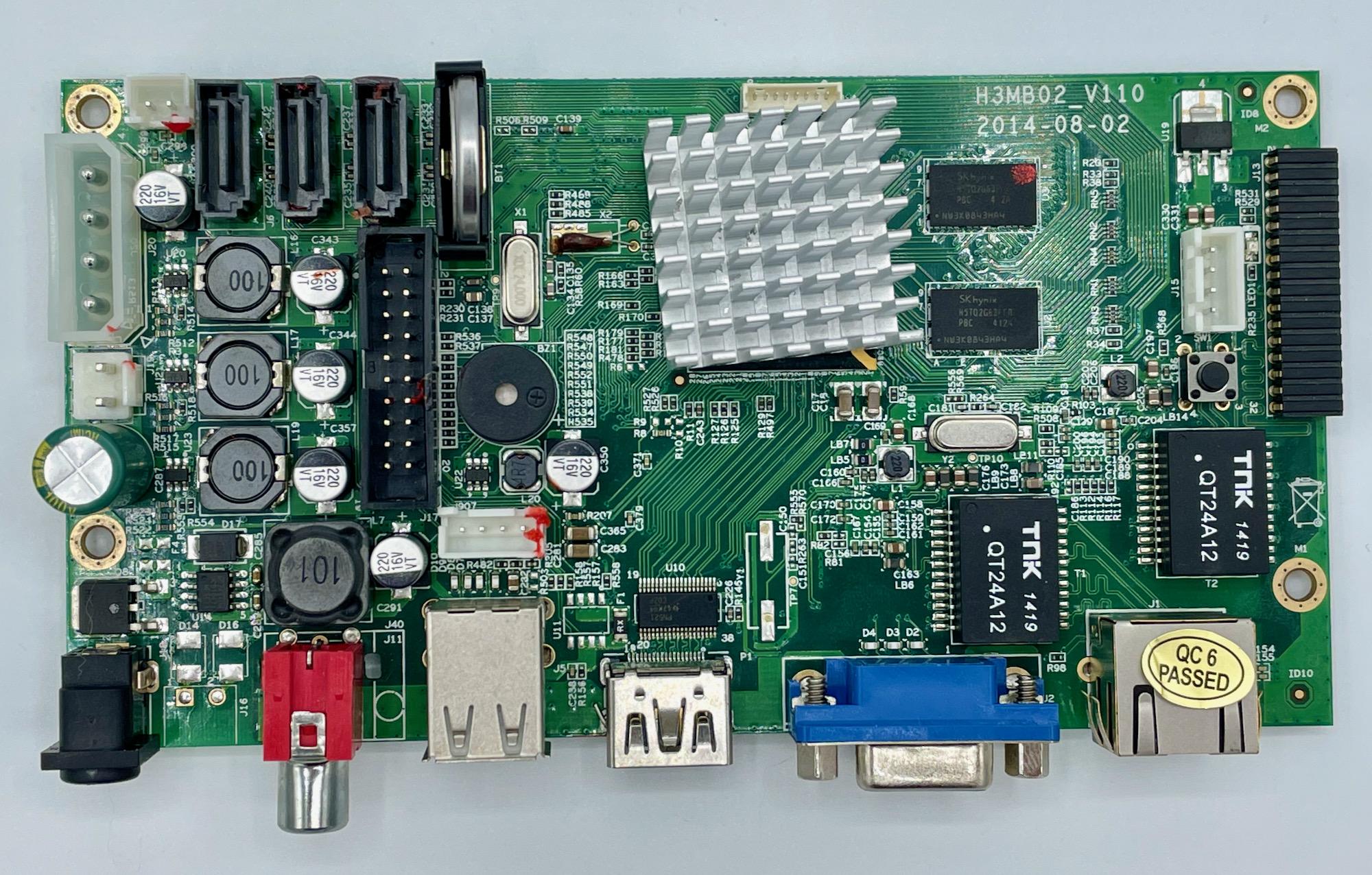
Markings:
- H3MB02_V110
- 2014_08_02
Chips:
- CPU: HiSilicon Hi3535 H.264 CODEC Processor (EDHS-PBGA-563) (brief datasheet PDF)
- U2, U3: DRAM: SKhynix H5TQ2G63FFR-PBC – 2Gb DDR3 SDRAM (“-PBC”: DDR3-1600, Commercial) (FBGA-96) (datasheet PDF)
- U4: Spansion S34ML01G200TFI000 – 1 Gb SLC NAND Flash Memory, 4-bit ECC, x8 I/O and 3V VCC (TSOP-48) (datasheet PDF)
- U7, U8 – Realtek RTL8211E – Integrated 10/100/1000M Ethernet Transceiver (QFN-48) (datasheet PDF)
- U10: TI TPD12S521 – Single-Chip HDMI Transmitter Port Protection and Interface Device (TSSOP-38) (datasheet PDF)
- U12 – SGMICRO SGM8903 – Capless 3Vrms Line Driver with Adjustable Gain – (TSSOP-14) (product page)
- T1: TNK QT24A12: ethernet magnetics for the external 1Gbps LAN port (specs PDF)
- T2: TNK QT24A12: ethernet magnetics for the internal ethernet port communicating with the daughter board’s 8-port switch (specs PDF)
Connectors:
- J1: RJ45 LAN ethernet (goes to the home network)
- J2: DB-15 VGA connector (actually, “DE-15”)
- J3, J4, J6: SATA connectors
- J5: USB-A USB 2.0 external connector
- J13: 32×2 (32 pins on 2 rows) right-angle header for the ethernet daughter board
- J14: 8×1 connector, unknown. Could it be JTAG? I didn’t try to investigate further.
- J15: 4×1 UART connector
- J17: 20×2 header for GPIOs (used for front panel LEDs, IR receiver)
- J18: Barrel Jack for DC48V power in
- J19: 2×1 PoE power connector
- J20: 4×1 Molex HDD power connector
- J21: 2×1 Fan power connector
- J40: RCA connector (mono) for Audio Out
- J907: 4×1 connector for the front panel external USB-A USB 2.0 connector
- P1: HDMI connector
PCB: PoE ethernet ports daughter board
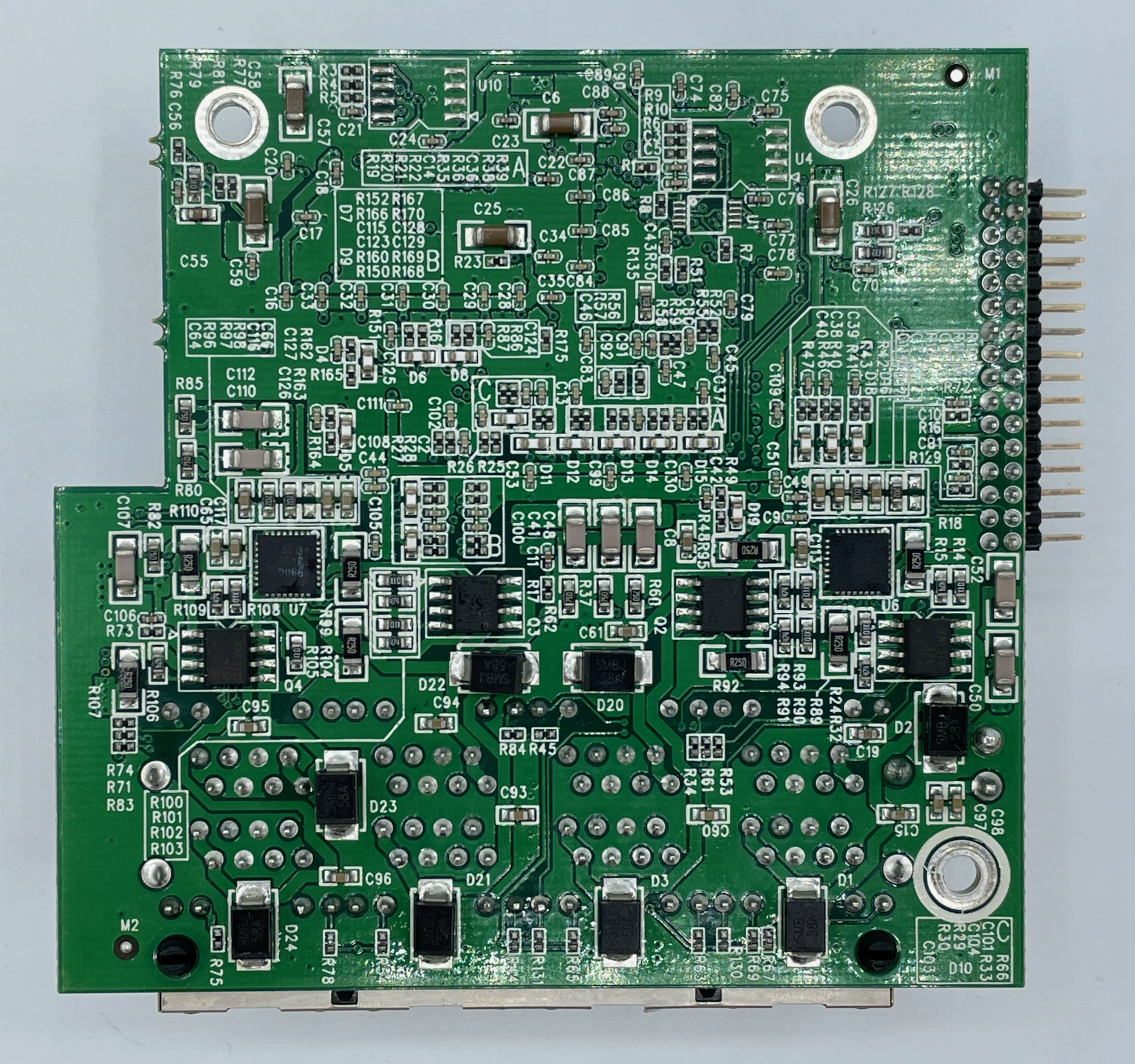
The daughter board is actually just a mini 8-port PoE (Power over Ethernet) ethernet switch. The stars of the show are the two Realtek RTL8306E switch controllers (in a cascading configuration I have to guess). 8 of the ports are exposed through the 8 RJ45 connectors, and one is used to communicate with the Hi3535 on the main board.
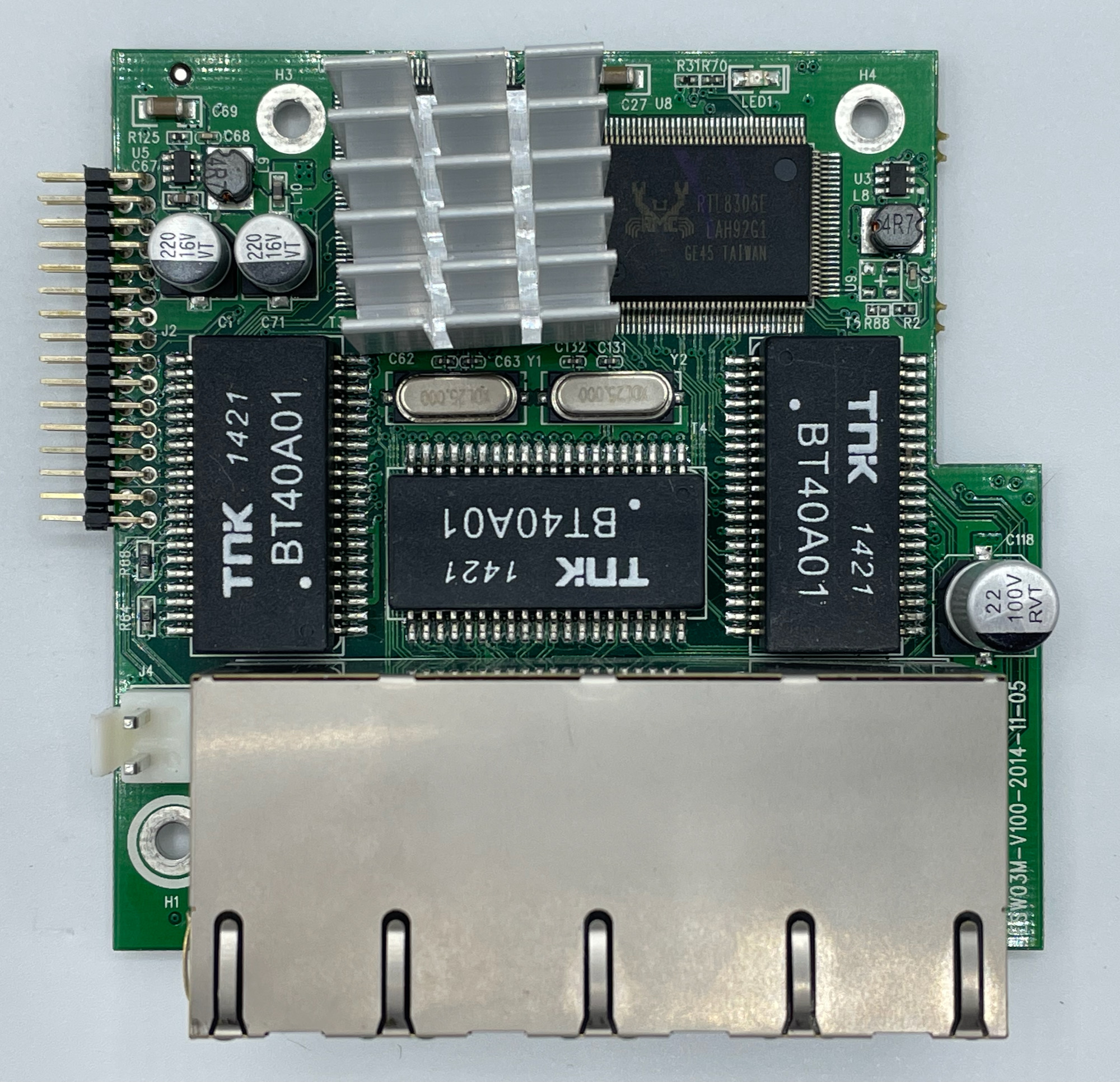
Markings:
- ESW03M-V100-2014-11-05
Chips:
- U2, U8: Realtek RTL8306E – Single Chip 6-Port 10/100Mbps Ethernet Switch Controller With Dual MII/RMII Interfaces (PQFP-128) (datasheet PDF)
- U6, U7: Maxim 5980G – Quad, IEEE 802.3at/af PSE Controller for Power-over-Ethernet (TQFN-32) (datasheet PDF)
- T3, T4, T5: TNK BT40A01 – 10/100 Base-T Quad Port Transformer (spec sheet PDF)
Front Panel
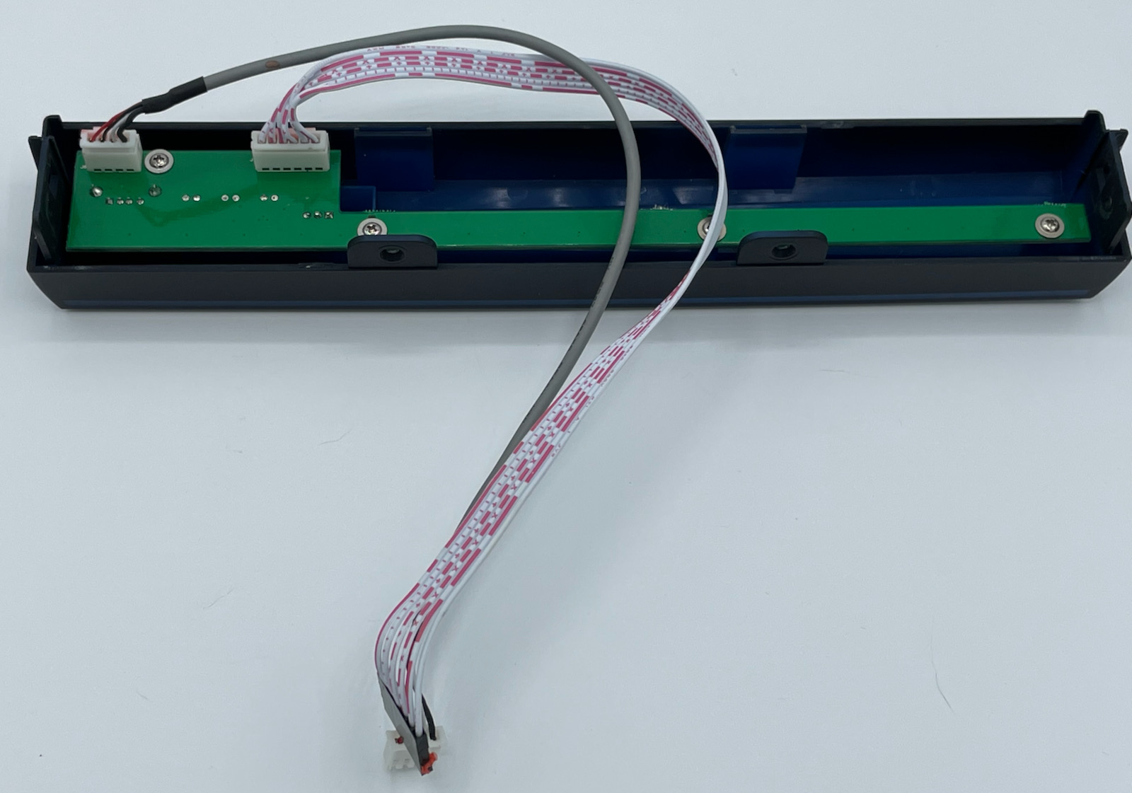
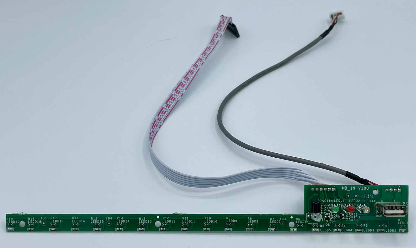
The front panel comes off the device easily after removing two screws securing it to the chassis on the bottom. Inside it lives a PCB that runs the whole length of the panel. It turns out there is a long “light band” at the bottom of the panel that glows light of various color (red, blue) under the device when some conditions are met (when you move the mouse for example). I guess it’s supposed to make it Look Cool maybe? The long PCB allows the designer to place LEDs all along the light band without any extra cabling (save for the cable going from the front panel to the main board).
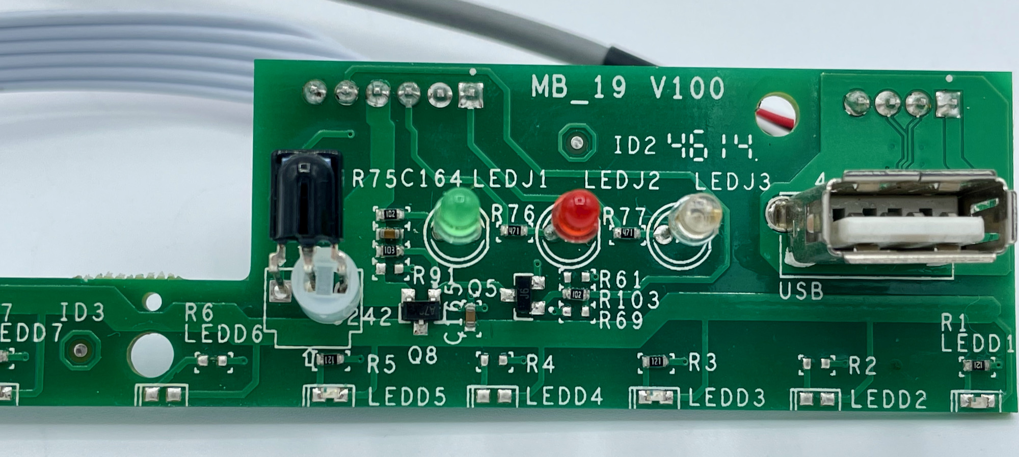
The PCB here is very simple: it holds the front USB connector, the three PWR/HDD/LAN LEDs, the IR receiver, and the series of LEDs for the light band at the bottom. The PWR led is permanently wired to VCC; HDD and LAN are driven by their respective signal coming from the main board; and all the light band LEDS (LEDD1 through LEDD19) are wired in parallel, driven by a pair of transistors Q5 and Q8 with a signal from the main board.
Note that out of the 19 light band LEDs, only 10 are populated (one every two). 19 LEDs is definitely a lot of bling and someone must have decided it was just a tad overboard after the PCBs had been locked in and cut the LED count in half 🙂
Markings:
- MB_19 V100
- 4614
Identifying the serial Console
Like so many of these embedded devices the board was suspected to have a serial port hooked to up the linux console. The 4-pin J15 header looked promising — 4 pins with one tied to GND is always a good start. Using my trusted Saleae Logic Analyzer I observed all four pins while starting the device and just like that, the serial port was confirmed on J15: GND, RX, TX, +5V.
Once connected to a standard Bus Pirate, the serial port shows the whole boot process revealing a U-Boot (2010.06) bootloader starting a Linux 3.4 kernel (Linux-3.4.35_hi3535). At the end of the boot process the console drops directly into a root shell, always nice! It will make exploring the device easier but is not necessary to take control over the device (as you will see in the Part 2 of this series).
Here’s the beginning of the boot log coming to the console upon startup:
U-Boot 2010.06 (Sep 24 2014 - 15:02:05)

NAND:  Check nand flash controller v504. found
Special NAND id table Version 1.36
Nand ID: 0x01 0xF1 0x80 0x1D 0x01 0xF1 0x80 0x1D
Block:128KB Page:2KB Chip:128MB*1 OOB:64B ECC:4bits/512Byte
128 MiB
Check spi flash controller v350... Found
Can't find a valid spi flash chip.
Can't find a valid spi flash chip.
*** Warning - bad CRC or NAND, using default environment

In:    serial
Out:   serial
Err:   serial
Hit any key to stop autoboot:  0

NAND read: device 0 offset 0x3ac0000, size 0x40000
 262144 bytes read: OK
dev 0 set background color!
jpeg decoding ...
<<addr=0x82000000, size=0x40000, vobuf=0x8a227000>>
mmu_enable
<<imgwidth=684, imgheight=456, linebytes=1376>>
decode success!!!!
decode jpeg!
dev 0 opened!
graphic layer 0 opened!

NAND read: device 0 offset 0x280000, size 0x380000
 3670016 bytes read: OK
## Booting kernel from Legacy Image at 82000000 ...
   Image Name:   Linux-3.4.35_hi3535
   Image Type:   ARM Linux Kernel Image (uncompressed)
   Data Size:    2358664 Bytes = 2.2 MiB
   Load Address: 80008000
   Entry Point:  80008000
   Loading Kernel Image ... OK
OK

Starting kernel ...

Uncompressing Linux... done, booting the kernel.
Booting Linux on physical CPU 0
Linux version 3.4.35_hi3535 (mdq@baichuan) (gcc version 4.4.1 (Hisilicon_v100(gcc4.4-290+uclibc_0.9.32.1+eabi+linuxpthread)) ) #6 SMP Wed Jun 24 11:30:14 CST 2015
CPU: ARMv7 Processor [414fc091] revision 1 (ARMv7), cr=10c53c7d
CPU: PIPT / VIPT nonaliasing data cache, VIPT aliasing instruction cache
Machine: hi3535
Truncating memory at 0x80000000 to fit in 32-bit physical address space
Memory policy: ECC disabled, Data cache writealloc
...
Similarities with Reolink NVRs
When I first worked on this NVR (especially on the firmware) I didn’t find many resources dealing with the topic so I did everything by hand. Later when writing up this post I bumped into Reolink, and it slowly became clearer: many of the Swann and Reolink devices share the same hardware, and a lot of the same software. It turns out Reolink used to be (I think) the Shenzhen Baichuan Security Technology, making hardware solutions for others to repackage and sell. Swann must have used and repackaged their hardware at some point.
The email in the ID line when the kernel boots up above is also a good indication 🙂
Linux version 3.4.35_hi3535 (mdq@baichuan) (gcc version 4.4.1 (Hisilicon_v100(gcc4.4-290+uclibc_0.9.32.1+eabi+linuxpthread)) ) #6 SMP Wed Jun 24 11:30:14 CST 2015In the case of the Swann NVR8-7300 it looks like a really really close cousin of the Reolink RLN8-410, both from a hardware design and layout, and from a firmware point of view.
If you have a Reolink NVR then you can keep on reading, a lot of things will apply to the Reolink world too (including the firmware manipulation tool I’ll describe in Part 2).
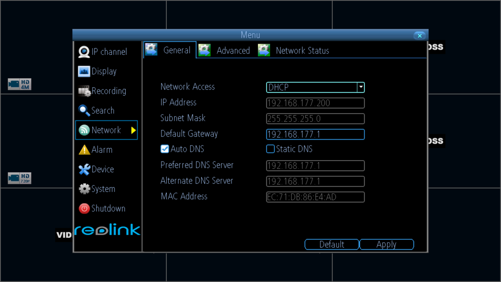
As an example, consider these two screenshots. One comes from my Swann’s NVR; the other one comes from the Reolink support page.
Wrapping-up
There you have it. The Swann NVR8-7300 is a standalone networked recorder for Swann IP cameras architected around a HiSilicon Hi3535 SoC. The Hi3535 is a domain-specific dual-core ARM Cortex-A9 chip with dedicated circuitry to do a lot of parallel H264 decoding/encoding. The box has 526MB of RAM, 128MB of onboard flash for the operating system and various bits of configuration, and an internal 2TB hard drive to store recorded footage. It runs an embedded Linux (with an older 3.4 kernel) with Busybox 1.16 covering most of the basic utilities. It interfaces with IP cameras through a 8-port PoE 100Mbps switch on a daughter board.
If you have questions on some aspect of this NVR please let me know in the comments.
Ready to patch it? Keep on reading to the next part, Part 2: Rooting the Firmware (coming soon!)