I just received a 12-port HyperDrive Gen 2 USB-C hub for my laptop and I couldn’t help but take a peek inside to see what it’s made of. Read on to see how it went.
The Device
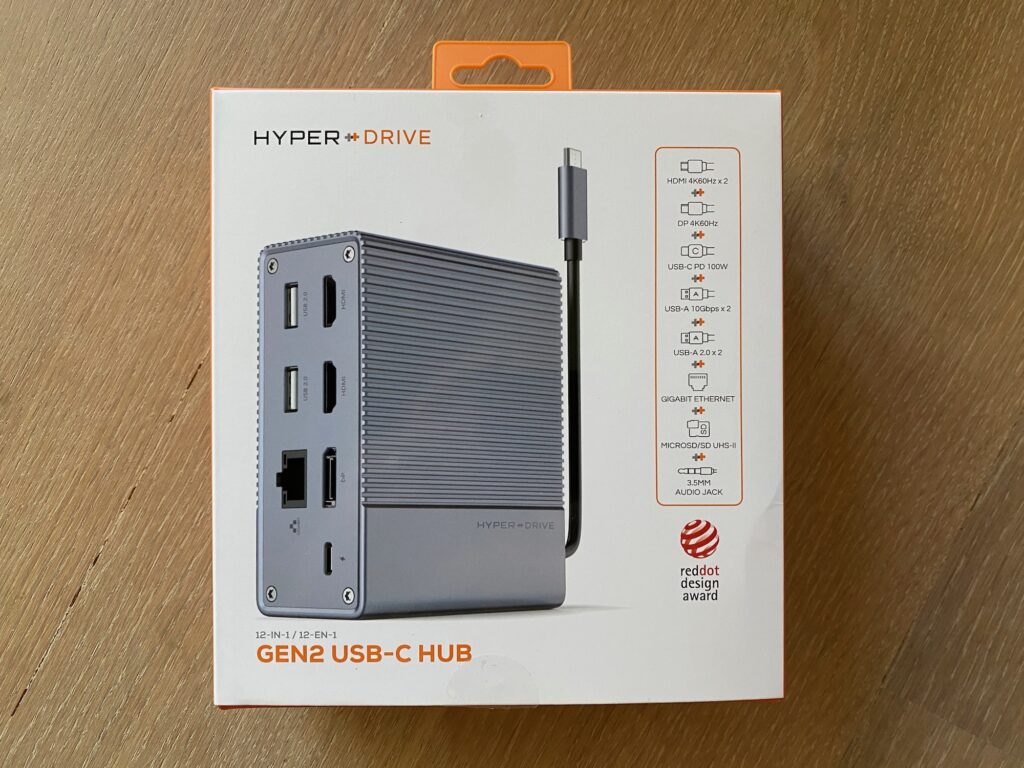
The device is a HyperDrive Gen 2 USB-C hub, 12-port version from HYPER by Sanho Corporation. Here’s their press release. As they’ve done in the past, they launched this product via a crowdfunding campaign on Kickstarter which met its target very quickly, and right now you can pre-order the device on indiegogo. It comes in 6-port, 12-port, and 18-port versions. Given all the ports and power delivery it could easily be called a docking station!
The specs for the 12-port version I have are as follows (from their press release):
- Consists of the following ports
- HDMI 4K60Hz HDR x2
- DisplayPort 4K60Hz
- USB-A 3.1 10Gbps x2
- USB-A 2.0 x2
- Gigabit Ethernet
- MicroSD UHS-II
- SD UHS-II
- 3.5mm TRRS Audio Jack (32-bit 384kHz)
- USB-C Power Delivery 100W
- Dimensions: 88.9 x 42.93 x 106.68mm (273mm cable) / 3.5” x 1.69” x 4.2” (10.75” cable)
- Weight: 480.81 g / 16.96 oz / 1.06 lbs
Unboxing
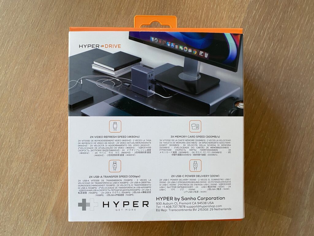
Not too much to see here. The box feels nice and tight. Inside is the hub sitting in a plastic insert and a tiny tiny piece of paper describing the ports (not pictured).
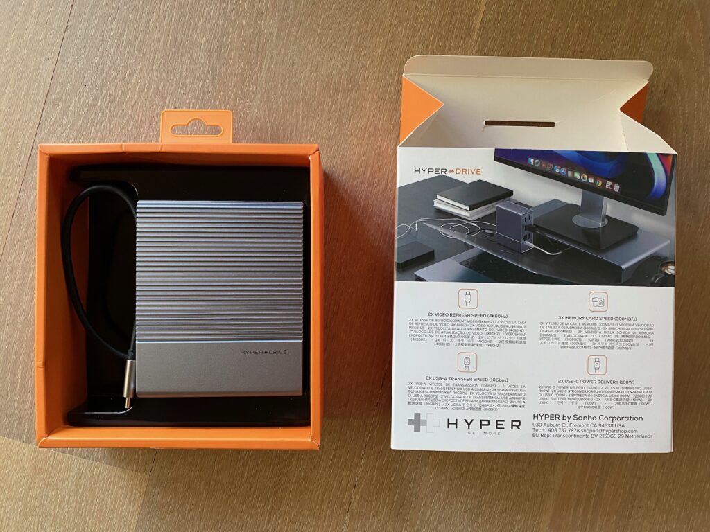
The hub itself feels really nice and solid. The aluminum enclosure appears to be machined precisely and at just over 1lb (480g) the hub has a nice dense feel to it. The unit is really tight, there is not a hint of play anywhere, and all the holes line up perfectly with their corresponding ports.
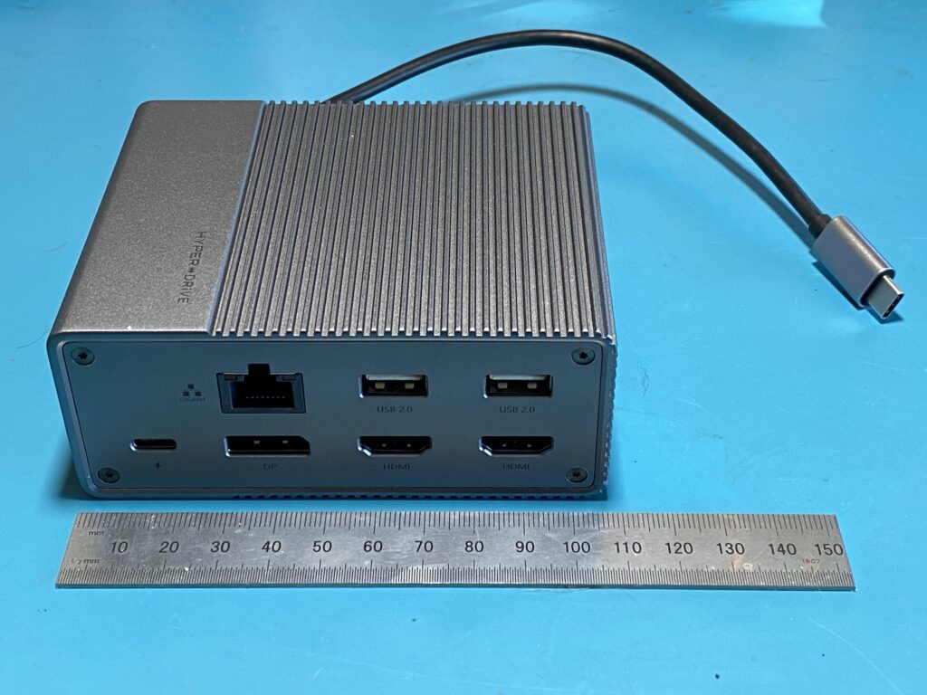
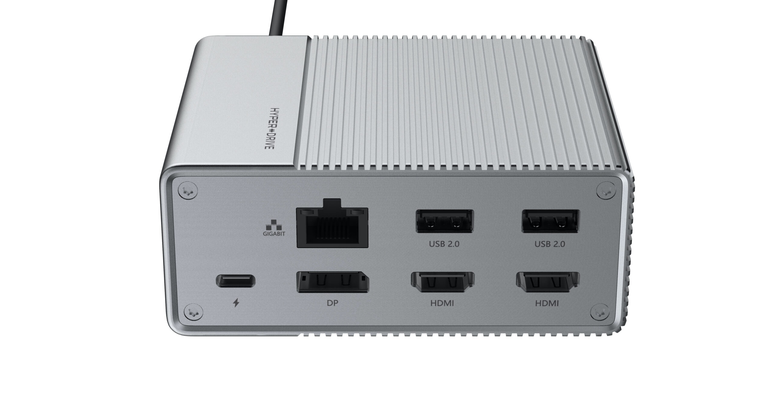
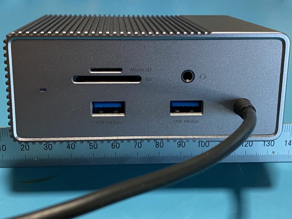
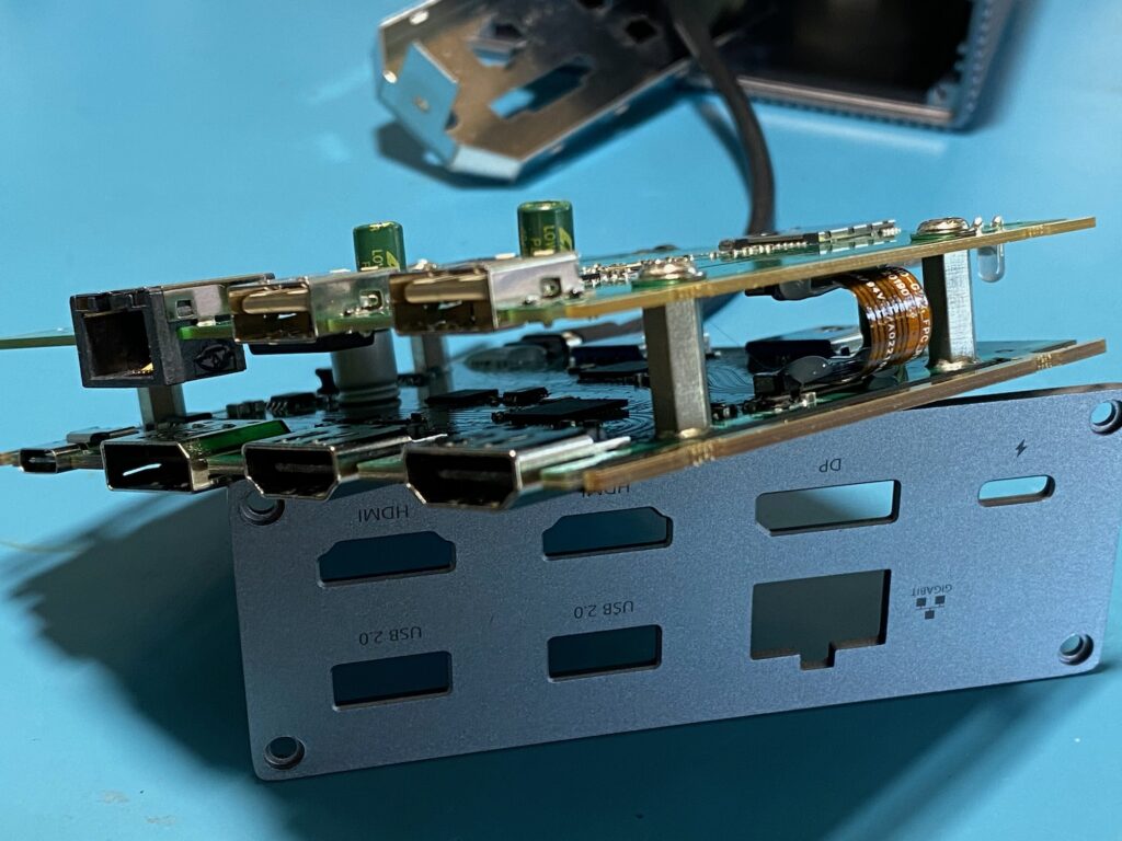
The front has 5 port (SD, MicroSD, 2x USB-A 3.1, 1 TRRS audio jack) and the cable to connect the hub to the computer. It also has the tiny power LED.
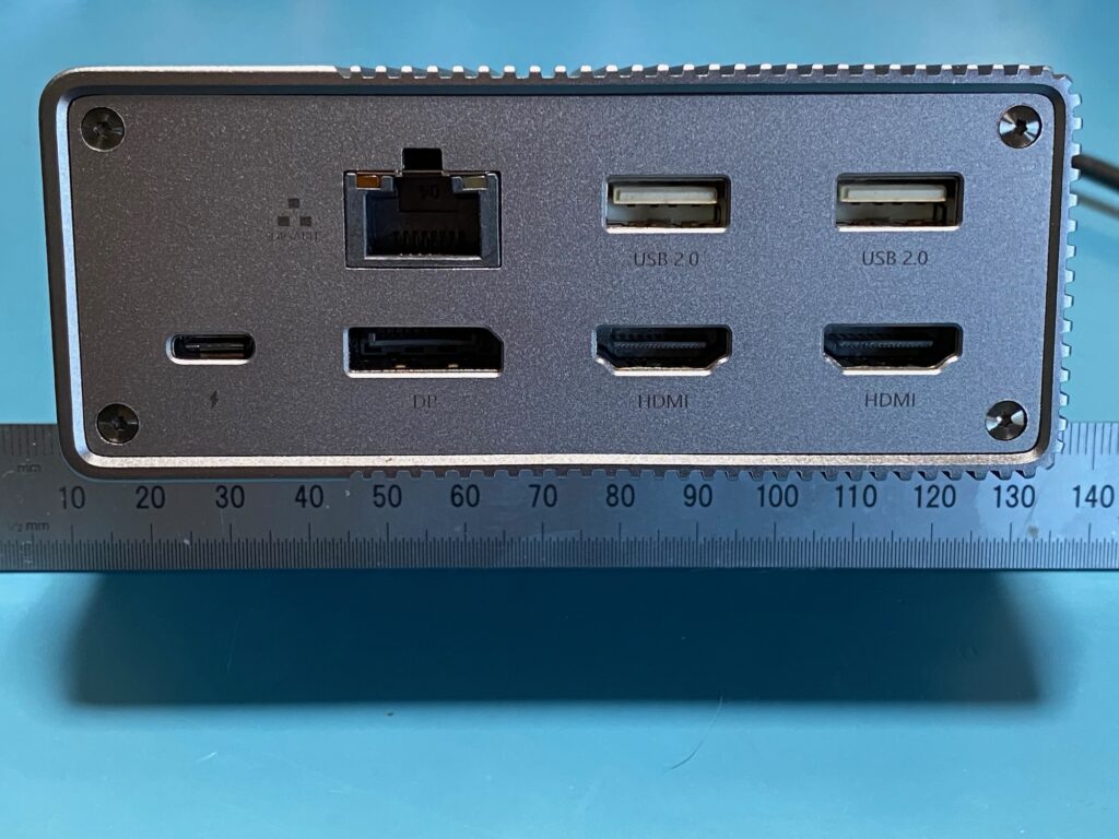
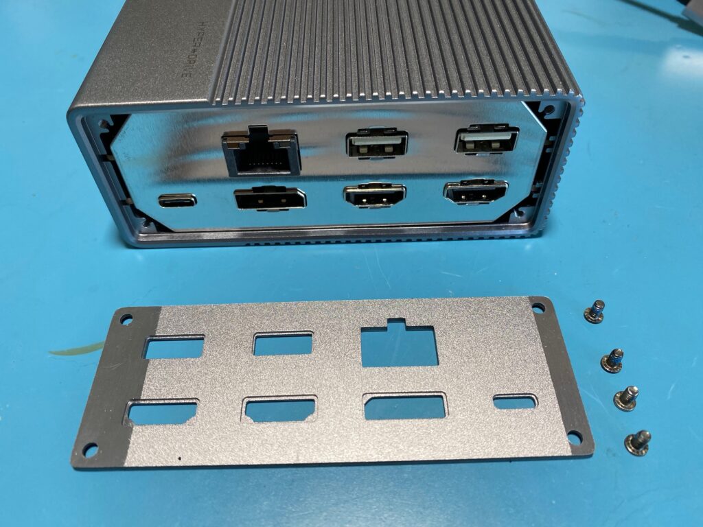
The back has 7 ports: Gigabit ethernet, 2x USB-A 2.0, 2x HDMI, 1x DisplayPort, and the USC-C PD power. Four torx screws can be found at the corners of the back plate.
Teardown
After removing the four Torx T6 screws from the back plate, the plate comes off relatively easily revealing some metal shielding around the back ports. The four screws have a bit of blue thread-locking fluid on them to prevent them from coming loose.
The internals are maintained in the enclosure by four rails on the sides and we can easily slide the whole thing out from the back. It turns out the circuitry is fully enclosed in a big metal shielding. The attached USB-C cable slides though the hole in the front of the enclosure but the USB-C connector at the end of the cable won’t fit through, so the enclosure will stay tethered to the rest of the device.
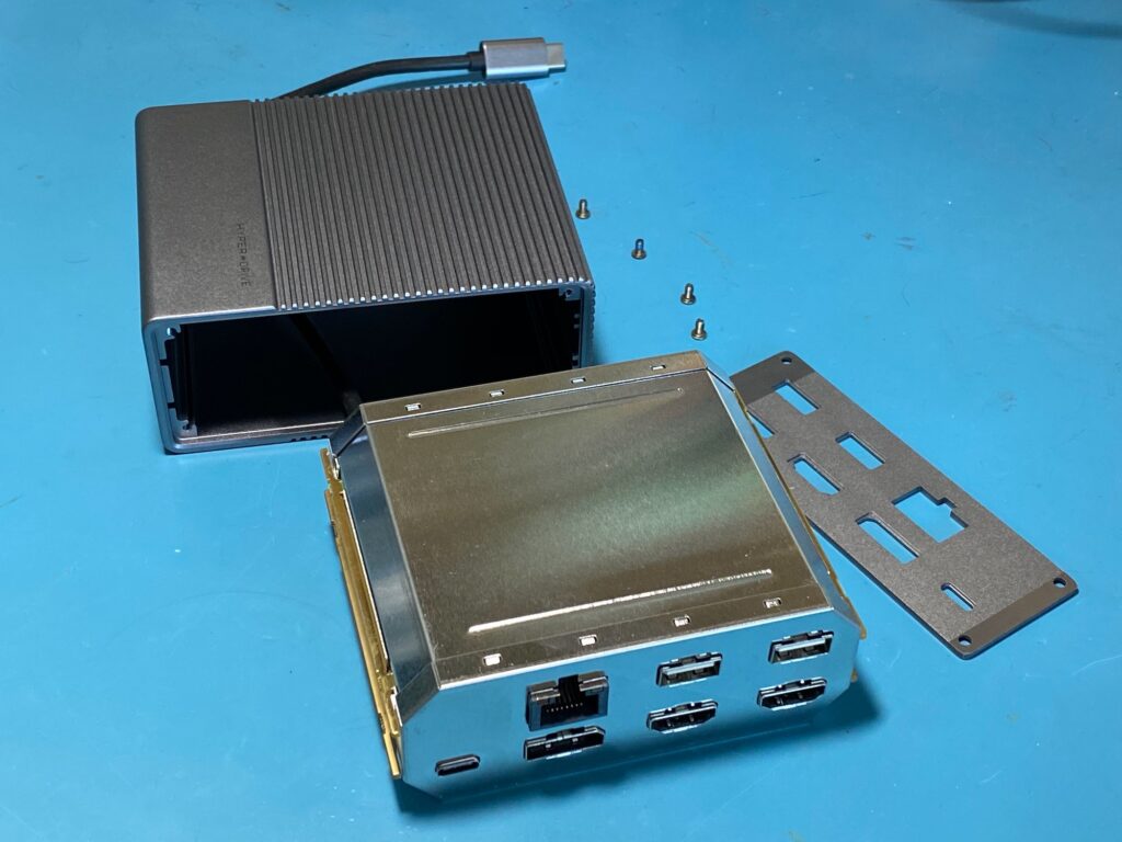
The metal shielding comes off reasonably easily: the front and back covers are lightly clipped onto the top and bottom parts, and after unclipping everything the four sides come apart without trouble.
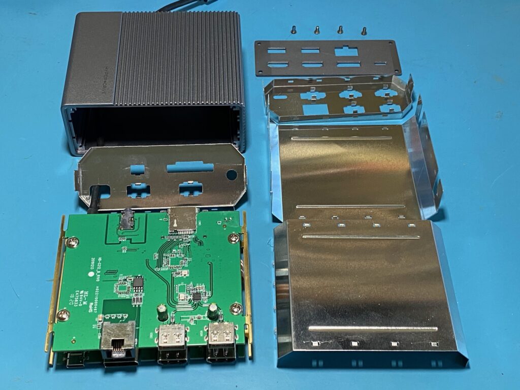
Now we see the true guts of the system: two individual PCBs with all the components and connectors directly mounted on them, screwed together over 0.5” metal standoffs and connected via what looks like a custom flex PCB. Components are mounted on both sides of each PCB. The sides of the PCBs have been coated in metal (copper?) and act as the rails to slide in the enclosure.
Once the four screws bolting the top PCB to the standoffs have been removed, we can see the interior sides of the PCBs. The attached USB-C cable and the two ends of the flex PCB have been glued for increased reliability.
One thing that jumped out at me was the curved traces. Such a change from 45deg angles, but I have to say it is quite pleasing to the eye 🙂
Chips
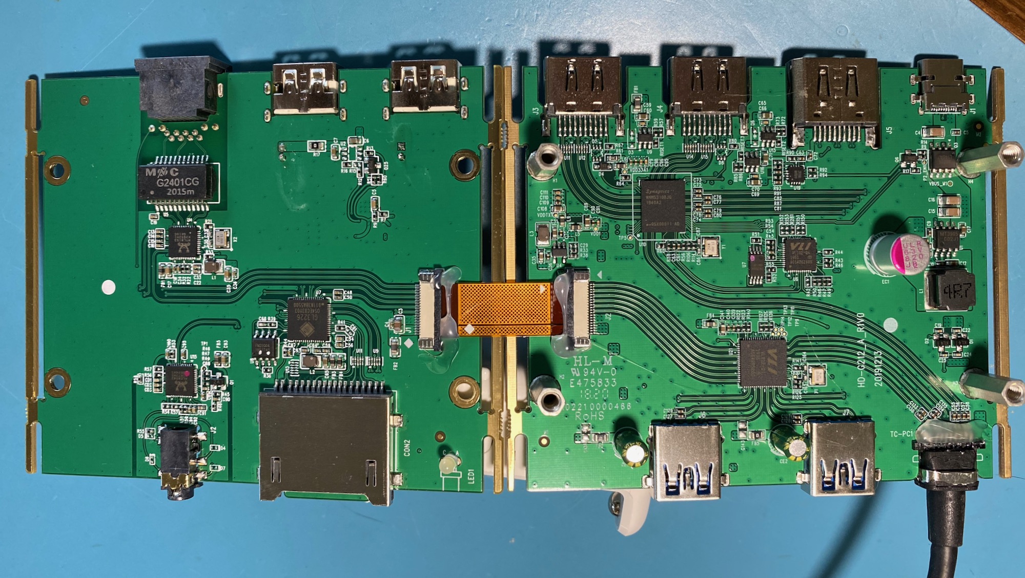
Top PCB
The top PCB has the ethernet port, the two USB 2.0 ports, the SD & microSD ports, and the audio TRRS port .
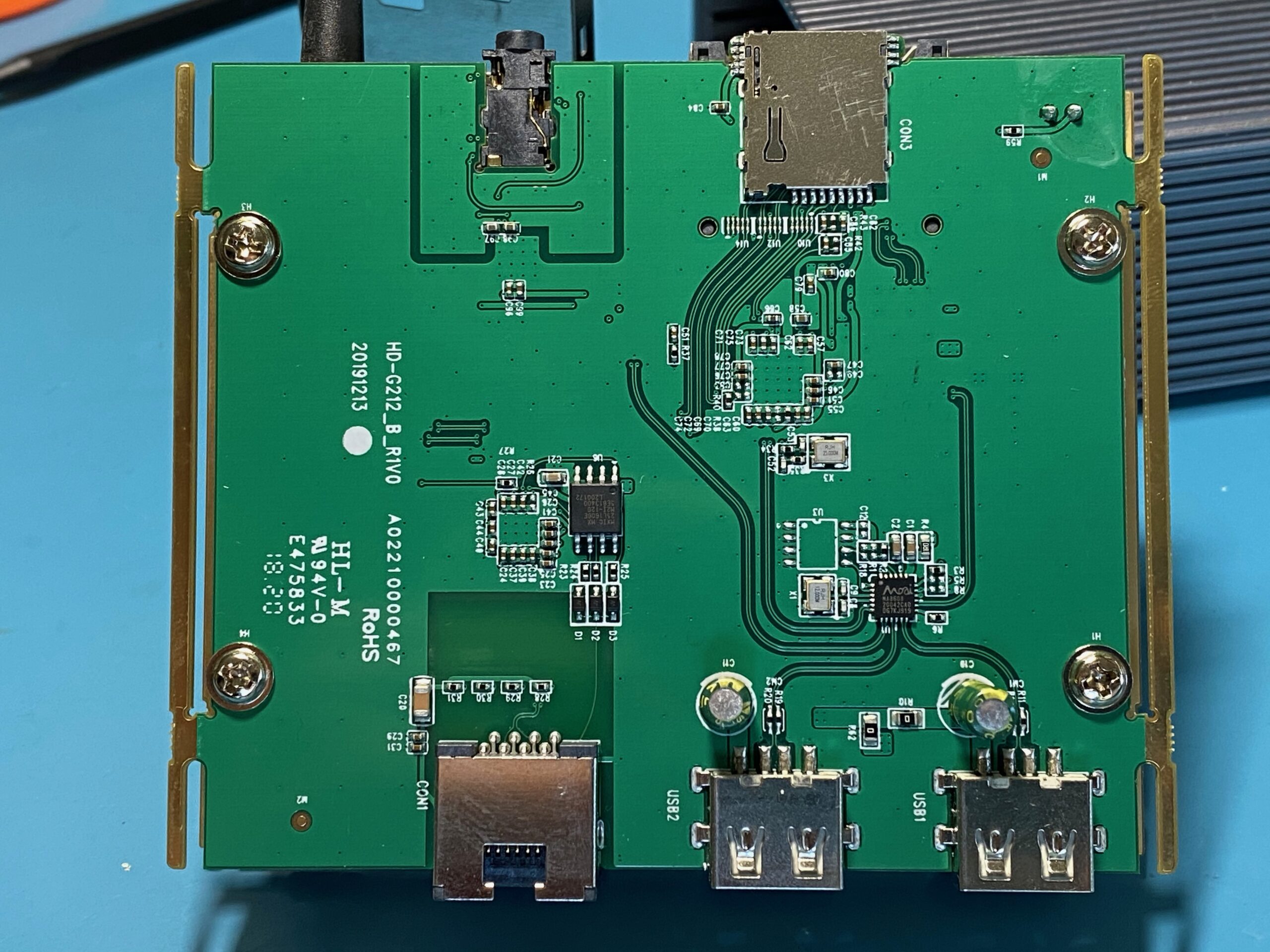
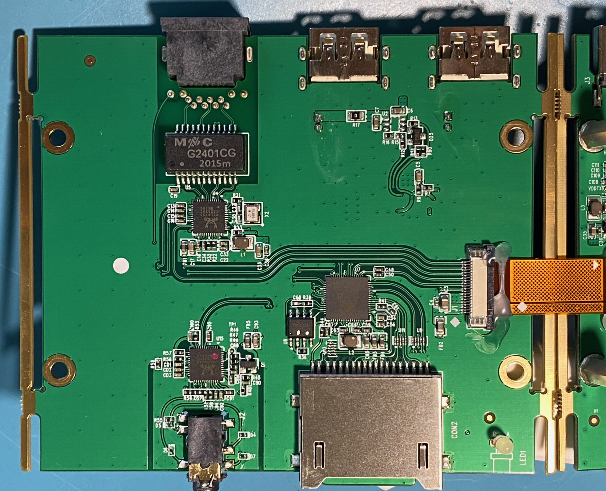
The supporting ICs are:
- U1 – MOAI MA8608 – USB 2.0 High Speed 4-Port Hub Controller (QFN-24) (datasheet)
- U4 – Realtek RTL8153 – Integrated 10/100/1000M Ethernet Controller For USB Applications (QFN-48 or similar) (no datasheet)
- U5 – Mentech G2401CG – 1000 Base-T Magnetics Transformer with IEEE 802.3ab Gigabit Ethernet (datasheet)
- U6 – Macronix MX25L1606E – 3V, 16M-BIT [x 1/x 2] CMOS Serial Flash Memory (SOP-8 200mil) (datasheet)
- U7 – Genesys Logic GL3226 – USB 3.1 Gen 1 Dual UHS-II Memory Card Reader Controller (QFN-64) (no datasheet)
- U8 – FM25Q04 – 4M-BIT Serial Flash Memory (SOP-8) (datasheet)
- U15 – Realtek ALC4042 – DAC 32Bit 384kHz (no datasheet)
Markings:
- HD-G212_B_R1V0
- 20191213
- A02210000467
Bottom PCB
The bottom PCB has the video block (2 HDMI, 1 DisplayPort), the 2x USB 3.1 ports, the USB-C PD port, and the upstream USB-C cable.
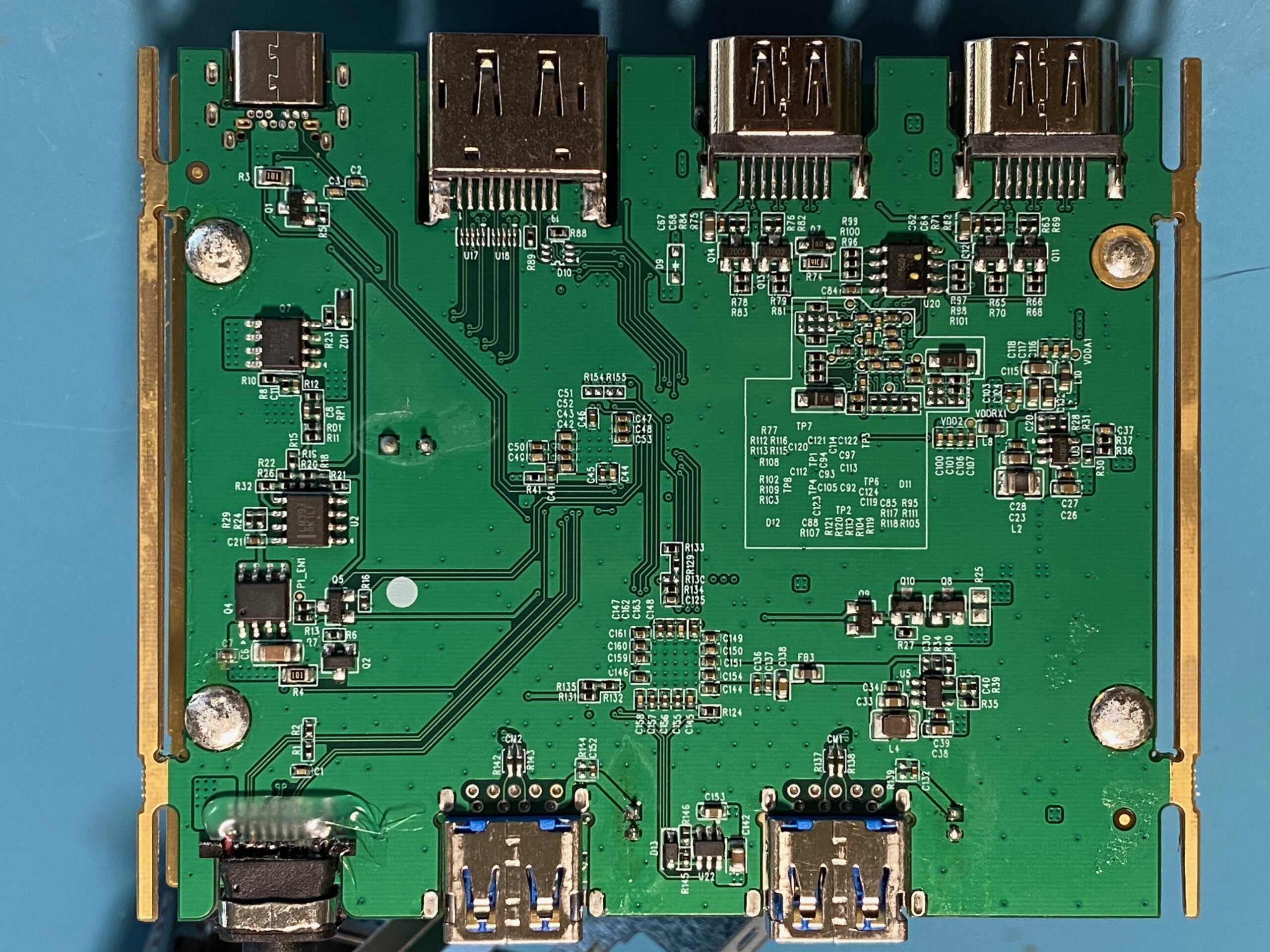
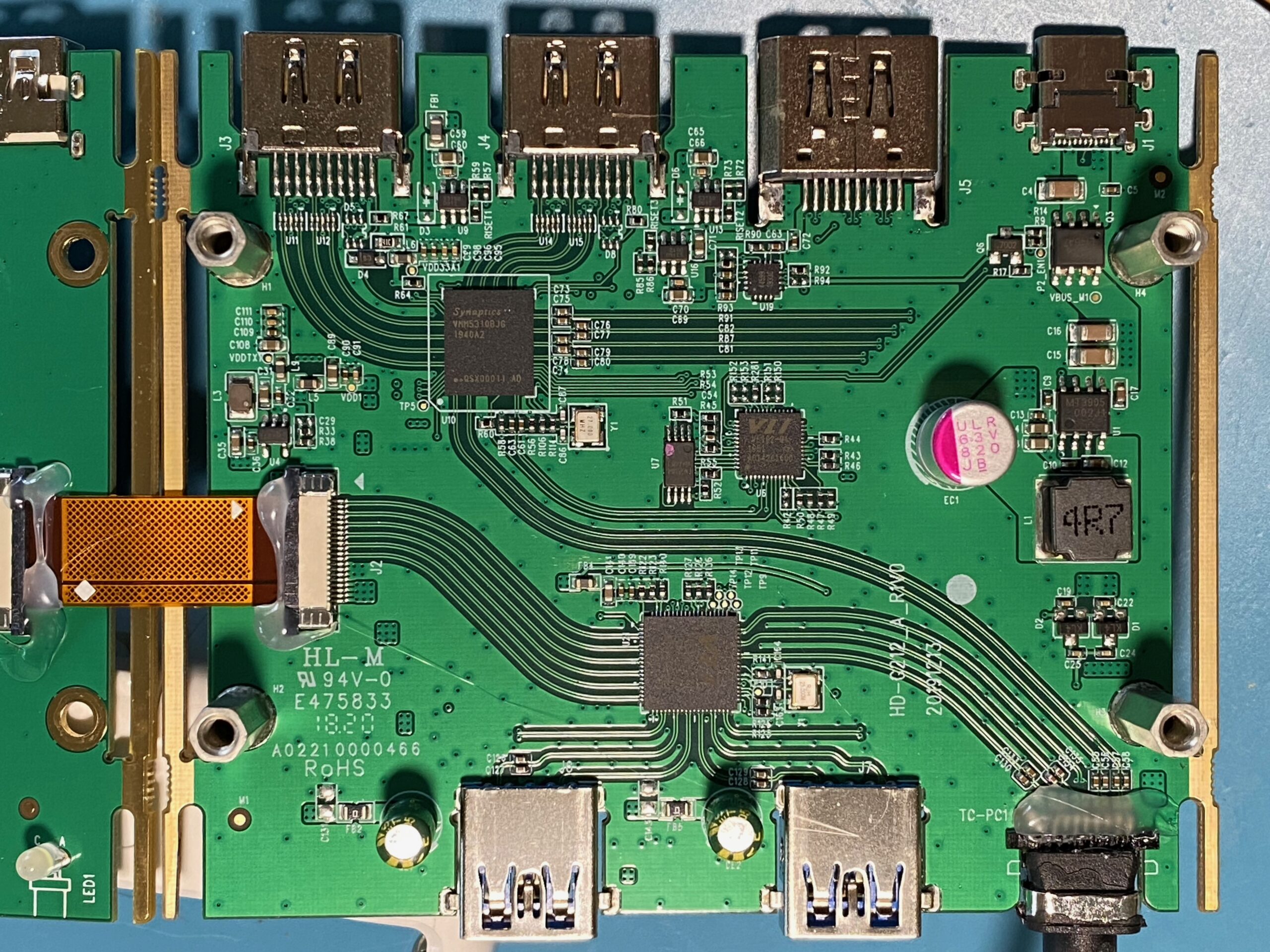
Supporting chips:
- U1 – MT3905 002J1 – ? (SOIC-8)
- U2 – TI LM393 – Low-Power, Low-Offset Voltage, Dual Comparator (SOIC-8) (datasheet)
- U6 – Via Labs VL102-Q4 – DP Alt-mode & PD 3.0 Controller for USB-C Devices (QFN-48) (datasheet)
- U7 – FM25Q04 – 4M-BIT Serial Flash Memory (SOP-8) (datasheet)
- U10 – Synaptics VMM5310BJG – ? Video Interface IC (BGA of sorts)
- U19 – SG Micro SGM44599 (most likely) – 4Ω, High Speed, Low Voltage Dual, DPDT Analog Switch (TQFN-16) (datasheet)
- U20 – FM25Q04 – 4M-BIT Serial Flash Memory (SOP-8) (datasheet)
- U21 – Via Labs VL822-Q7 – USB 3.1 Gen2 Hub Controller
Markings:
- HD-G212_A_R1V0
- 20191213
- A02210000466
Conclusion
The HyperDrive Gen2 USB-C hub is a very nice little device with impressive specs. You can tell a lot of attention has gone into the details and the build quality. It was very easy to open it up and tear it down, as well as putting it back together (whew!). Now the moment of truth will be how well it performs once I plug it into the laptop.. We will see!
When other manufacturers switch to VL103 or FL7102/FL7112, HyperDrive still insists on using VL102. How touching
Thank you for taking the time and effort to perform the teardown and document it. This answered some of the curious questions I had regarding which components were inside. Your write-up was more helpful than the official documentation!